Clock generation
Every computer needs a square wave clock signal that drives the processor through a program. In a simple processor like the 6502 this works as follows: in the first clock cycle the next opcode is fetched from memory, in the next cycle(s) it is decoded and the operands are fetched from memory and in the following cycle(s) the operation is executed (calculated) and the result is written back to memory.
A normal MOS 6502 processor can be clocked up to 1 MHz, a 6502A up to 2 MHz and a 6502B up to 3 MHz (yes, MHz not GHz!).
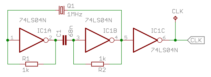
First I decided to use a classical quartz oscillator built with three 74LS04 inverter gates. Two inverters together with the quartz, two resistors and a capacitor form a "series resonant gate oscillator" that oscillates with the frequency of the quartz and a third inverter buffers the output signal. This and other configurations can be found in the following application notes (search the internet for "crystal ttl oscillator circuits" for more information about this topic):
Euroquartz Application Notes: Oscillator Circuits
Linear Technologies Application Note AN12: Circuit Techniques for Clock Sources
Intel Application Note AP-155: Oscillators for Microcontrollers
Later on i replaced this circuit with a simple quartz oscillator module which does the same job but is much easier to use:

(Image source: Wikipedia )
.jpg)
This module outputs a 1 MHz TTL square wave signal that can be directly fed into the ICs of our microcomputer.
Schematic
Breadboard construction
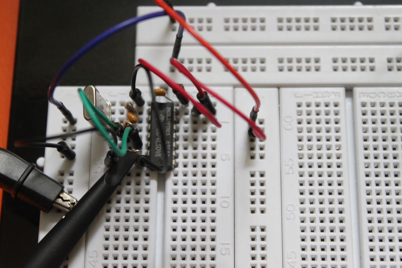
I began the construction in the top left corner, connected everything to power and checked if the clock signal shows up at pin 6 of the 74LS04 IC.
Measurements
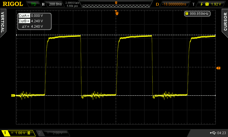
As we can see, this is by no means a perfect square wave signal. There's lots of ringing and the signal only slowly goes up to 4.24 V. But for driving an ancient 6502 microprocessor system this is sufficient.
PCB
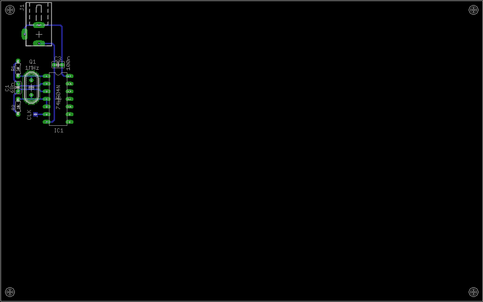
Layout and route individual modules of your circuit independently. By doing that you can move them around and connect the various modules later on. So even if you only have a small part of your circuit completed and you don't know where to place it, that shouldn't stop you from starting to layout the PCB for this module.
These pictures show the progression from this first clock generation module until the whole computer system is completed. Keep in mind that the first few versions are more like sketches that change significantly over time. The complete schematics and PCB layouts (final and all versions) can be found in the eagle subfolder of the GitHub repository of this project .