EEPROM and a first program
If you really want get the feeling of the 80s, then you should use EPROMS of the 27C series and an UV EPROM eraser device like the ones shown here:
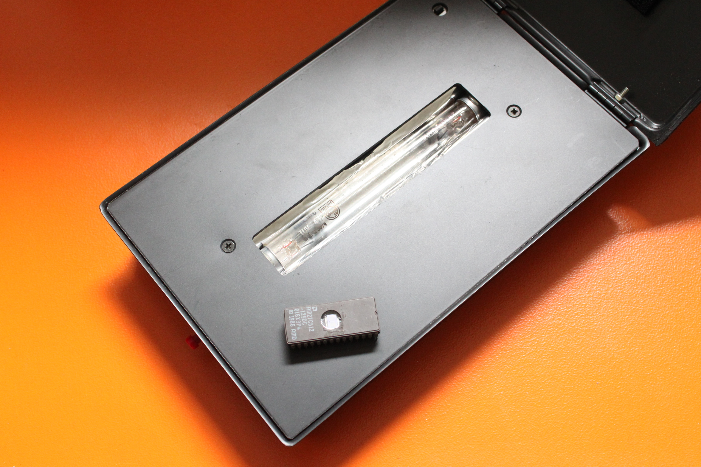
But since it takes quite some time to erase an EPROM (> 15 min.) and during software development you need to reprogram the EPROM very often, this quickly becomes a tedious process.
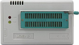
So it's better to use a modern parallel CMOS EEPROM like the AT28C256 from Atmel and a modern programmer. The most versatile and best priced product for hobbyists IMHO is the MiniPro TL866 from the Chinese company Auto Electric .
If you are working under Linux, you can control MiniPro from the command line. Check out the great programming tool written by Valentin Dudouyt on GitHub: https://github.com/vdudouyt/minipro .
Since you need to continuously move the EEPROM between the programmer and the circuit, it's best to use a ZIF socket for the microcomputer circuit (this is the same socket that is used in the programmer above).
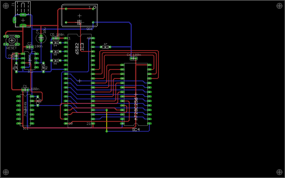
Schematic
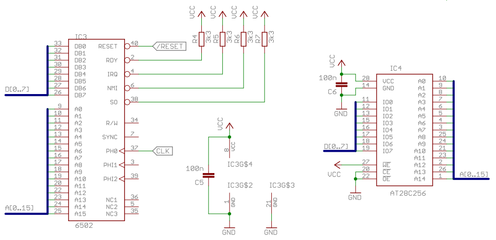
The AT28C256 is a 32 kB (32k*8) EEPROM and is connected to the data and address buses. Since we currently have no address decode logic, !CE and !OE are wired directly to ground. Because of this, the EEPROM appears at the addresses $0000 - $7FFF and $8000 - $FFFF.
Breadboard construction
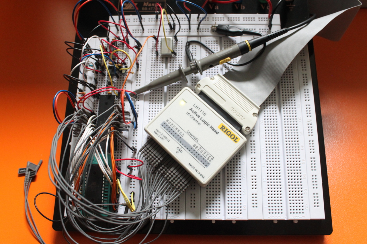
The EEPROM and the logic analyzer are attached to the microprocessor. The lines D0 to D7 of the analyzer are connected to the data bus and the lines D8 to D15 are connected to the lower 8 bits of the address bus (A0 to A7). You can also see that i've replaced the oscillator circuit with a compact oscillator module.
Software
I'm using the CC65 assembler/compiler/linker suite to develop my 6502 programs. The first step is to create a configuration file that describes the memory map and the various sections in these memory areas. A first simple version looks like this:
MEMORY
{
  ROM: start=$8000, size=$8000, type=ro, define=yes, fill=yes, file=%O;
}

SEGMENTS
{
  CODE: load=ROM, type=ro;
  VECTORS: load=ROM, type=ro, offset=$7ffa;
}
And here is our first program. After a reset the CPU jumps to the location loop. Here it enters a simple loop that continuously loads $12 into the accumulator and jumps back to loop.
          .setcpu "6502"
          .segment "VECTORS"

          .word   loop
          .word   loop
          .word   loop

          .code
loop:     lda
          jmp loop
This compiles into the following rom:
00008000 a9 12 4c 00 80 00 00 00 00 00 00 00 00 00 00 00
00008010 00 00 00 00 00 00 00 00 00 00 00 00 00 00 00 00
*
0000fff0 00 00 00 00 00 00 00 00 00 00 00 80 00 80 00 80
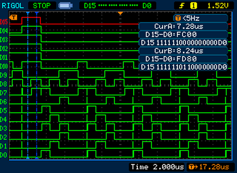
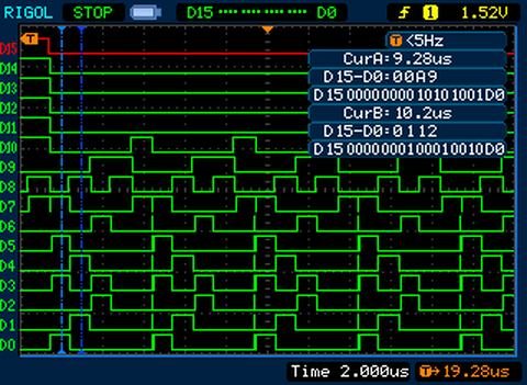
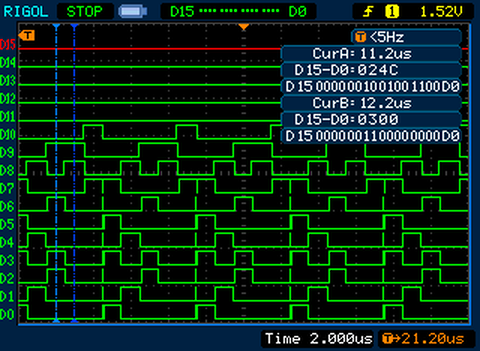
00010000Measurements
The following diagrams are recorded with a logic analyzer and show the bus activity after a reset. D0 to D7 show the bits of the data bus and D8 to D15 show the lower 8 bits of the address bus (A0 to A7). Cursor A and B show decoded bus values for two consecutive memory reads. As you can see the following addresses and memory values are accessed:
| Address | Value | Operation |
| FFFC | 00 | Reset vector lo |
| FFFD | 80 | Reset vector hi |
| 8000 | A9 | LDA |
| 8001 | 12 | |
| 8002 | 4C | JMP |
| 8003 | 00 | Jump address lo |
| 8004 | 80 | Jump address hi |
| 8000 | A9 | LDA |
| and so on... | ... | ... |

PCB
Lots of changes:
- Now using two layers
- Replaced the discrete oscillator circuit with an oscillator module
- A jumper wire (you can spend hours on re-routing your layout to avoid the need for jumper wires...)
Tip: If you're aiming for home fabrication and need jumper wires, simply use an additional layer for them and increase the drill size of the vias.